
Hello, I am Paul David.
Semiconductor professional focused on Wide Band Gap (WBG) power transistors
Experienced in device engineering, process integration, test and electrical characterization
About Me
I am an experienced Device Engineer with a demonstrated history of working in the power semiconductor industry. Skilled in device engineering, characterization, process integration, and management. Proven expertise in devising and implementing solutions to optimize performance, process, and reliability by electrical characterization. Adept at collaborating with cross-functional teams and providing valuable insights for process improvement and product development. Proficient in data analysis of various data sets to provide data driven guidance.

Developing With a Passion While Exploring The World.
With a strong background in semiconductor device testing, characterization, and process integration, I bring innovative solutions, meticulous attention to detail, and a passion for advancing technology. I thrive in dynamic environments where collaboration and innovation drive success. As a dedicated and experienced professional, I am eager to contribute my expertise to the semiconductor industry and make a lasting impact.
Work Experience
Product Engineer - Manufacturing, Device Engineering
Durham, NC
- Responsible for leading a high impact design change which would result in a substantial decrease in product defectivity and increase device robustness to switching stresses.
- Proposed various projects for Yield and Quality improvements by analyzing real-world performance data and studying workflow processes.
- Compiled weekly KPI report related to complete power product portfolio manufacturing performance.
- Owned and monitored two highest volume Automotive MOSFETs at North Carolina Fab, resolving fabrication, yield and quality issues.
Before Wolfspeed, I was as a Senior Staff Device Test Engineer – Process Integration at NexGen Power Systems, where I was instrumental in setting up and maintaining electrical characterization equipment for GaN-on-GaN discrete devices. Based at both the Santa Clara, CA, and Syracuse, NY locations, I worked closely with cross-functional teams, including product engineering and device engineering, to ensure efficient testing procedures. I had developed and maintained comprehensive documentation on tool use and maintenance, enabling the smooth operation of testing processes. I had also been part of many internal task forces in assessing and improving performance and reliability of products in NexGen’s 700V and 1200V product portfolio.
Prior to joining NexGen Power Systems, I served as a Device Engineer at GV Semiconductors in San Jose, CA. I successfully set up and maintained an electrical characterization lab for GaN power semiconductor products, both in wafer and packaged form. Through advanced and standard measurements and design of experiments, I correlated device process parameters to electrical data and real-world performance. I actively contributed to the layout and processing of GaN-based products, providing feedback for improved reliability and performance. Moreover, I played a pivotal role in the reliability testing of GaN devices, crucial for their qualification in mass production.
Sr. Staff Device Char. Engineer - Process Integration
Santa Clara, CA & Syracuse, NY
- Setup and training of electrical characterization equipment for packaged and wafer level devices for product, device & integration engineering teams leading to fast cohesive cycles of learnings from bare wafer to application modules.
- Managed and mentored technicians & junior engineers to perform accurate routine wafer characterization ensuring >90% utilization and high engineering data throughput.
- Oversaw ~0% down time operation and maintenance of >$300k in test equipment and implemented strategic upgrades to align engineering capabilities with company goals.
- Managed process module development of 1200V device portfolio to improve manufacturability and yield.
- Analyzed large electrical wafer sort data and inline fab data to drive yield improvement & correlated electrical parameters to process experiments for product performance improvements.
- Worked extensively in Process Integration team to investigate device physics related phenomenon affecting transistor performance and reliability by developing non-standard characterization tests.
- Achieved multiple device performance milestones by rigorous analysis of metrology and electrical characterization data & collaborating with epi, process, reliability & device engineering teams.
- Completely digitized and automated in-house business processes using productivity tools such as MS Power Automate to improve data organization, access and traceability.
Sr. Device Engineer
San Jose, CA
- Setup and maintained electrical characterization lab for GaN HEMT power transistors products in wafer and packaged form.
- Performed advanced and standard measurements (such as RDS(on), Gate Charge, Capacitance, etc.) on GaN based D-mode and E-mode devices for deeper understanding of device behavior, parameter extraction and modelling.
- Contributed by providing characterization, layout, and process feedback of GaN based devices leading to improved reliability and performance.
- Contributed to reliability testing of GaN devices crucial to device qualification for mass production.
- Achieved expansion of in-house characterization capabilities by design and implementation of specialized fixtures/techniques while saving company >90% cost of readily available solutions.
- Acted as a liaison between application, technical marketing and fab teams to drive customer-centric product improvements.
- Developed techniques related to Gate Charge measurement of power devices in sub nC range and an alternative method without the use of a current limiting FET.
Technical Skills

Software
- JMP Data Analysis and Scripting
- Layout Editor
- Python, C/C++
- Power Automate (MS)
- Lab View Programming
- Electrical Characterization software – ACS Basic, Clarius, EasyTest Expert, EasyTest Navigator

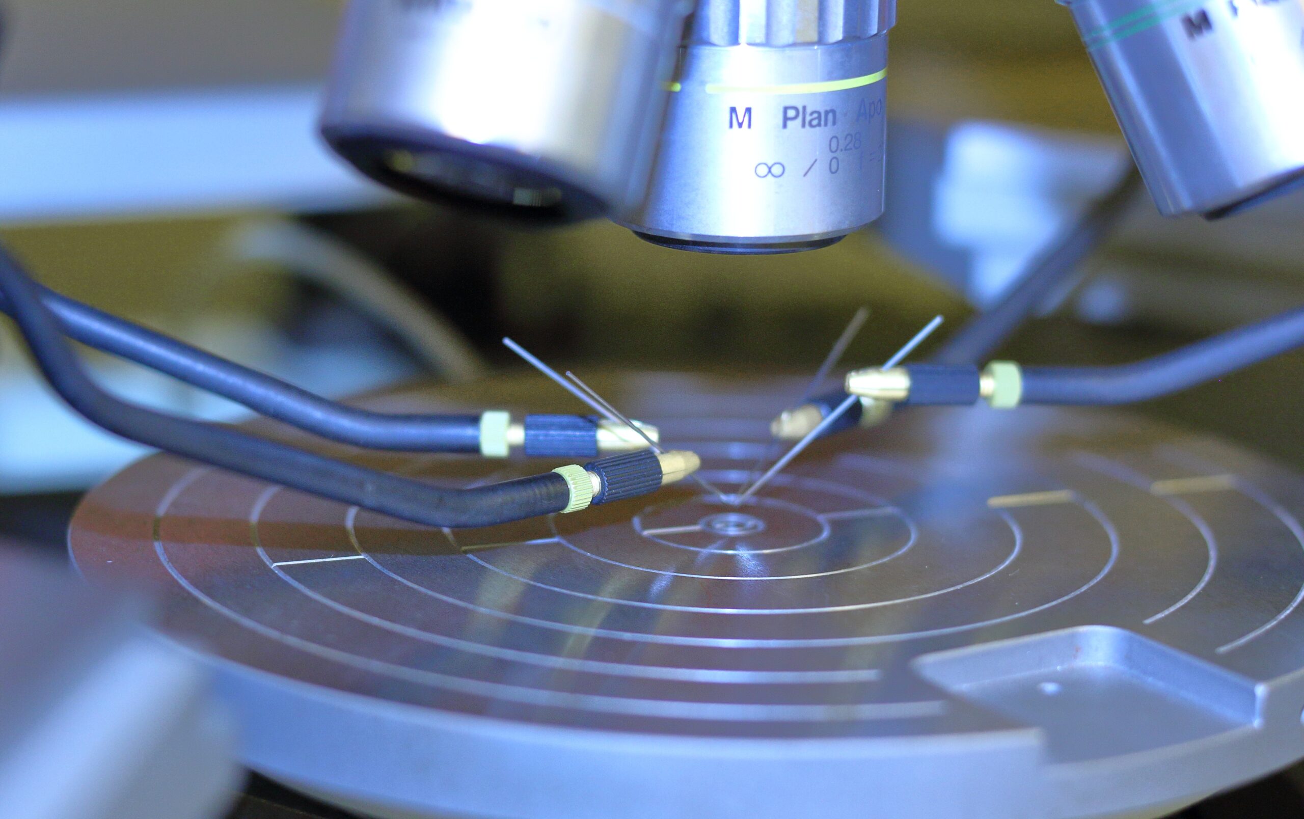
Electrical Characterization
- Wafer Prober measurement (Manual/Automated)
- HV/HC AC-DC-Pulsed Measurements on wafer and packaged devices
- Dynamic Measurements (Ciss, Coss, Crss, Rg)
- Gate charge measurement
- Electrical Parameter Analyzer (4200, B1505/6)
- Thermal measurements

Process
- Process Integration
- E-Beam lithography
- Photo lithography
- ILD deposition
- Dry plasma etch
- Wet etch
- Physical Vapor Deposition
- Chemical Vapor Deposition
- Metrology – SEM, TEM, AFM, EDX, FIB
Soft Skills
- Problem-solving
- Project management
- Effective communication
- Delegation
- Time management
- Effective feedback
- Team motivation
- People management
- Knowledge management
- Team management
Academic Experience

August 2010 – May 2014
Bachelor of Science in Nanoscale Engineering
Concentration in Energy and Environmental Applications
Notable Projects:
ZnO(1-x)S(x) as an Alternative Buffer Layer for CIGS Thin Film Photovoltaics
Effect of CVD growth parameters on Electronic and Physical properties of Carbon Nanotubes
August 2014 – May 2017
Master of Science in Nanoscale Engineering
Concentration in Nanoelectronics
Notable Projects:
Fabrication and electrical characterization of DNA based PN Diode